Performance and production.
Everything we develop has to deliver against these, often conflicting, objectives. Our architecture and materials are based on advances in semiconductor engineering, while the production process leverages solid-state fabrication of integrated circuits.
- Multiple alloy systems providing linearity and loss characteristics unattainable for transistors.
- Demonstrated operation >300ºC.
- Arc-free designs can support hundreds of volts with a miniaturized air-gap.
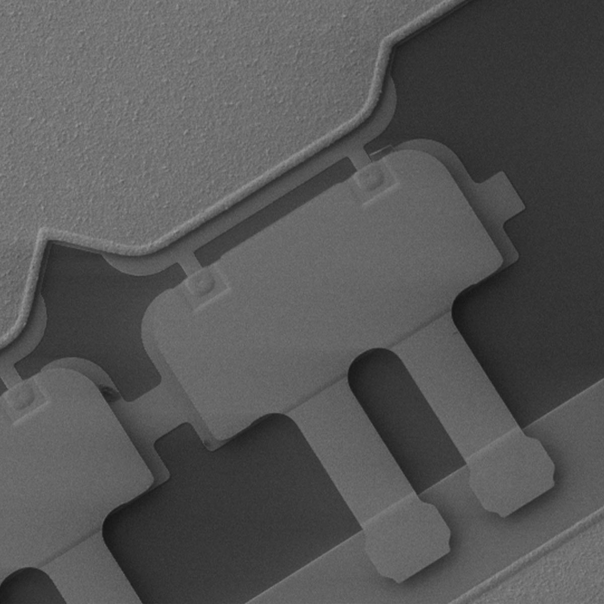
- Tiny actuators exhibit switching speed of <10μs and are relatively immune to shock & vibration.
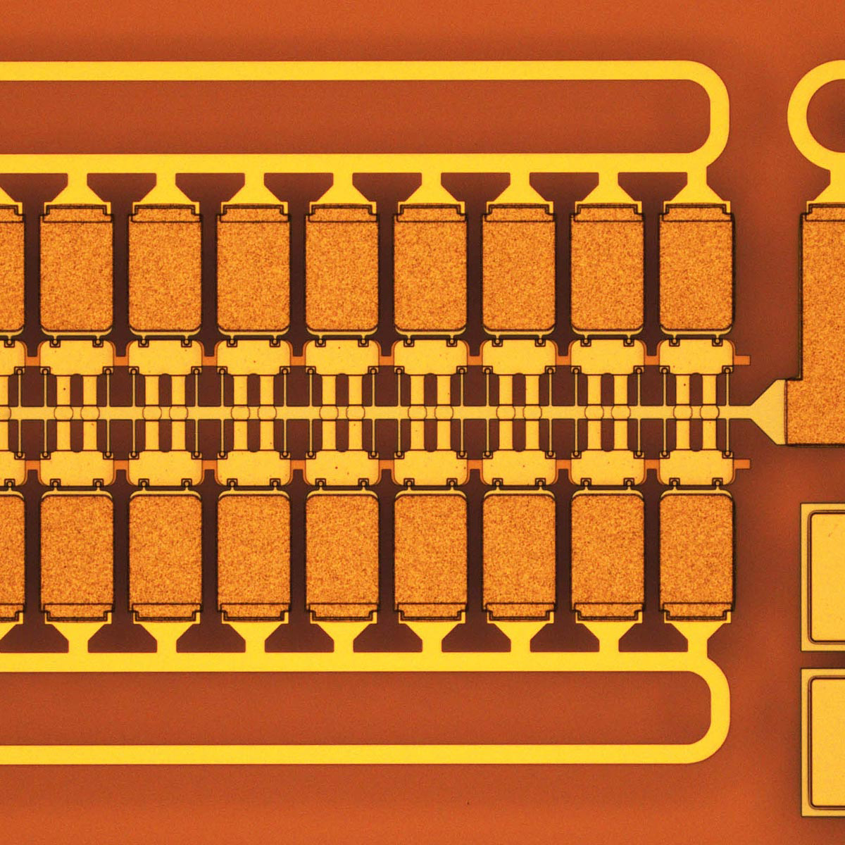
- The small size enables the creation of massive arrays.
- The array layout is flexible to allow for infinite product combinations.
- Can scale designs to >1000V and >50A.
- Enables both low-power and high-power RF, AC and DC switches using the same unit cell and process.
Through-Glass-Via Packaging
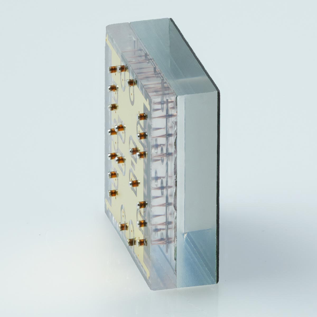
- Reduces size of traditional wire-bond packaging by >60%.
- Compared to silicon, metal-on-glass delivers lowest loss, highest linearity performance.
- Drastically reduced package parasitics to enable designs >50 GHz.
- Hermetically sealed environment enables the Ideal Switch to achieve billions of reliable operations.
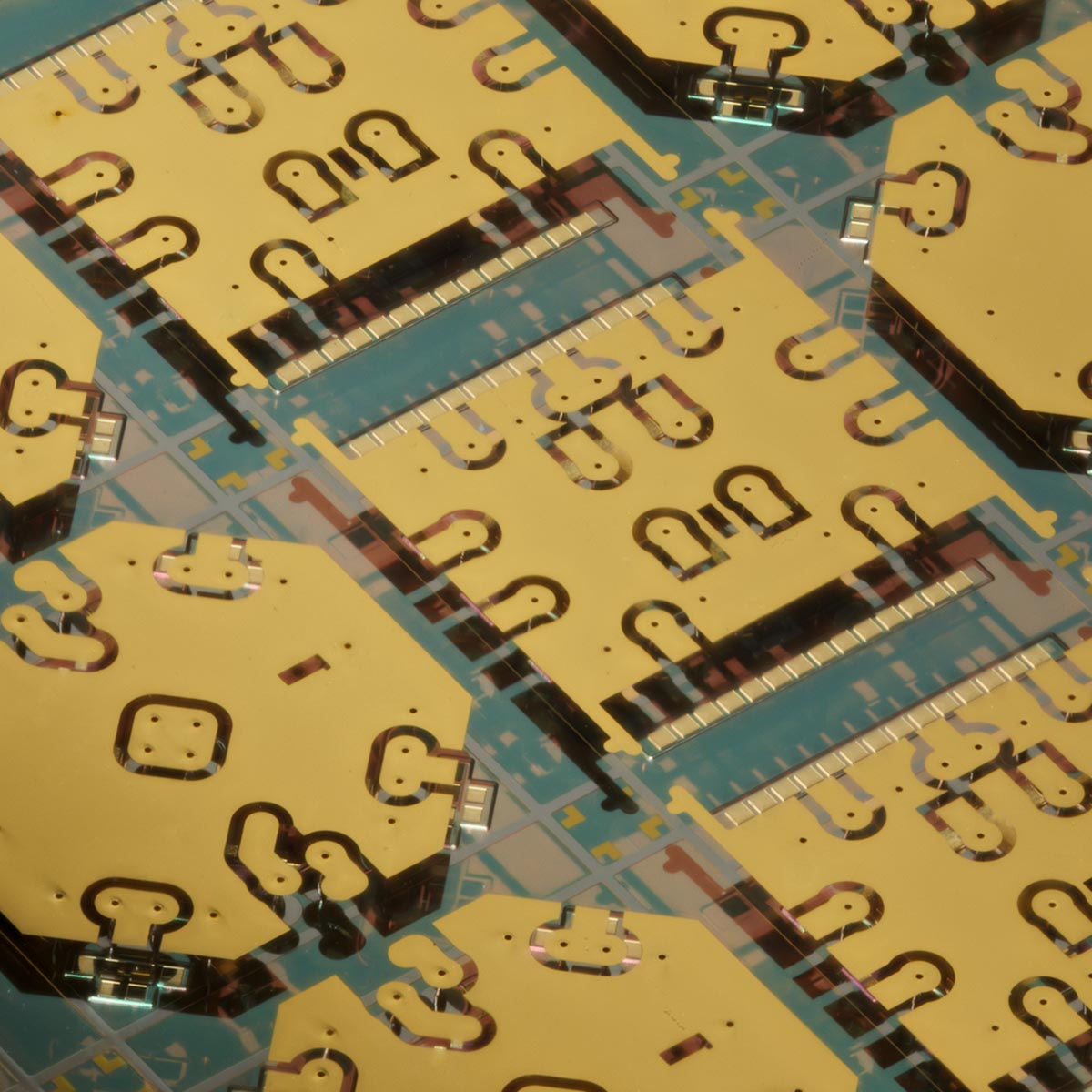
- 8-inch (200mm) glass wafer fabrication, using standard semiconductor processing equipment.
- Thousands of die on single wafer, chip-scale package from 16mm2 down to <1mm2.
- Roadmap to “System-on-Glass.” Integrate passives and other structures directly on glass with switches to create ultra-miniaturized RF subsystems.
