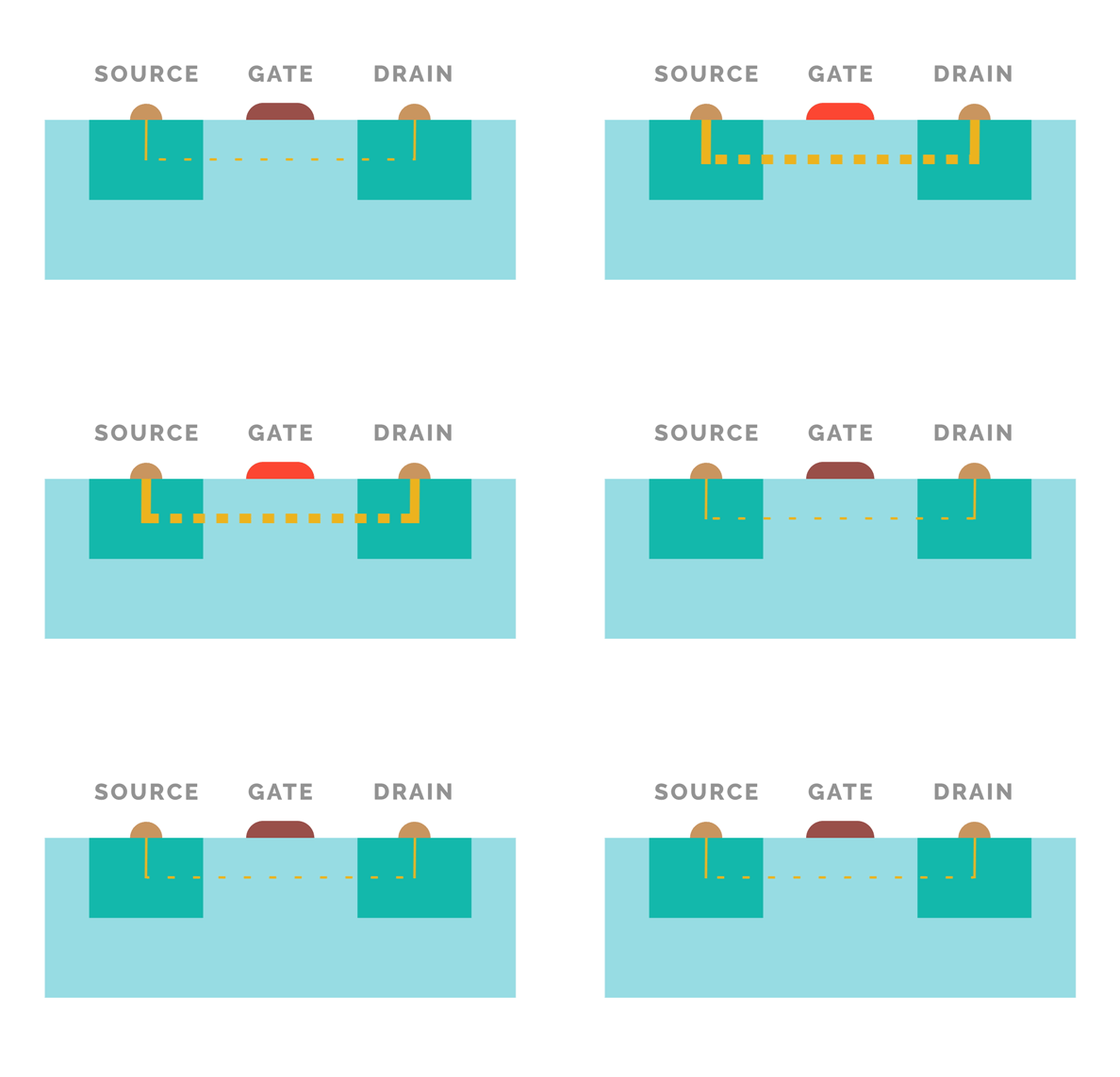
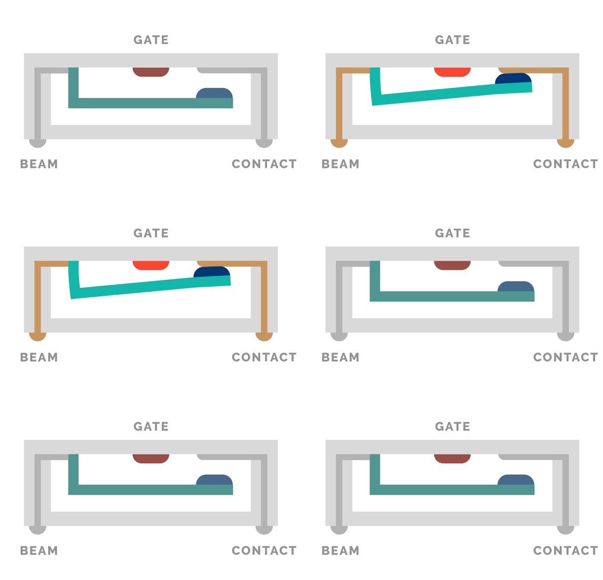
BEAM
• Proprietary alloys
• High temperature capable
• Decades of life
CONTACT
• Low resistance
• Billions of operations
• No stiction
GATE
• Electrostatic = low power
• No charging
FROM UNIT CELL TO CELL ARRAY
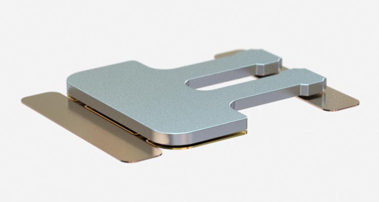
Simple cell design makes it very small – 50μm x 50μm – and easy to pack in dozens or hundreds of switches on a die.
SCALABLE PRODUCTS
Configurable in series and/or parallel designs to create an infinite number of product configurations.
THROUGH-GLASS-VIA
PACKAGING
Packaging hermetically sealed in a miniaturized chip-scale package for superior RF performance.
SCALABLE MANUFACTURING
Simple 14-layer process and 8” wafers enables high-volume and low-cost manufacturing.
VERSATILITY
World’s first standardized Process Design Kit for a MEMS switch. Shorter design cycles and faster time-to-market for new products.
BEAM
• Proprietary alloys
• High temperature capable
• Decades of life
CONTACT
• Low resistance
• Billions of operations
• No stiction
GATE
• Electrostatic = low power
• No charging

FROM UNIT CELL TO CELL ARRAY
Simple cell design makes it very small – 50μm x 50μm – and easy to pack in dozens or hundreds of switches on a die.
SCALABLE PRODUCTS
Configurable in series and/or parallel designs to create an infinite number of product configurations.
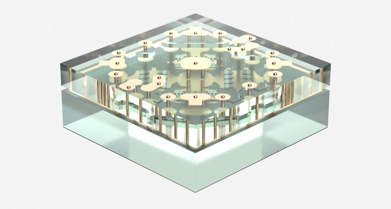
THROUGH-GLASS-VIA
PACKAGING
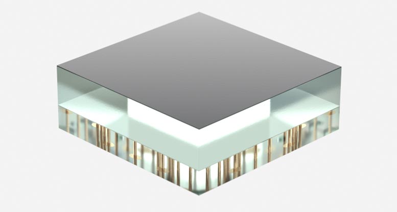
Packaging hermetically sealed in a miniaturized chip-scale package for superior RF performance.
SCALABLE MANUFACTURING
Simple 14-layer process and 8” wafers enables high-volume and low-cost manufacturing.
VERSATILITY
World’s first standardized Process Design Kit for a MEMS switch. Shorter design cycles and faster time-to-market for new products.
BEAM
• Proprietary alloys
• High temperature capable
• Decades of life
CONTACT
• Low resistance
• Billions of operations
• No stiction
GATE
• Electrostatic = low power
• No charging
FROM UNIT CELL TO CELL ARRAY
Simple cell design makes it very small – 50μm x 50μm – and easy to pack in dozens or hundreds of switches on a die.
SCALABLE PRODUCTS
Configurable in series and/or parallel designs to create an infinite number of product configurations.
THROUGH-GLASS-VIA
PACKAGING
Packaging hermetically sealed in a miniaturized chip-scale package for superior RF performance.
SCALABLE MANUFACTURING
Simple 14-layer process and 8” wafers enables high-volume and low-cost manufacturing.
VERSATILITY
World’s first standardized Process Design Kit for a MEMS switch. Shorter design cycles and faster time-to-market for new products.
